The difference between Passive Optical Network (PON) and Active Optical Network (AON)


Passive optical network (PON) and active optical network (AON) are two access technologies for building DWDM and CWDM backbone networks in FTTH systems. Both have their own advantages, so what are the main differences between them? How should we choose?


Signal Distribution

The difference in signal distribution is the biggest difference between passive optical network (PON) and active optical network (AON). In a passive optical network (PON), there is a situation where optical fiber bundles are shared between users, while in an active optical network (AON), each user has an independent optical fiber chain, and there is no shared bandwidth between each other , Therefore, relatively speaking, the passive optical network (PON) system does not run as fast as the active optical network (AON), and it is more difficult to troubleshoot when a fault occurs.


Cost

As we all know, the main sources of network costs are power supply equipment and maintenance costs. It can be seen from the above that the passive optical network (PON) has no other power supply equipment except for both ends, and requires less maintenance and no power supply; while the active optical network (AON) mainly uses power supply equipment for network transmission, so relatively In general, the cost of active optical network (AON) is higher than that of passive optical network.


Coverage

Passive optical networks (PONs) typically only cover distances up to 20 kilometers, while active optical networks (AONs) can cover distances up to about 100 kilometers. In other words, users in the passive optical network (PON) must be closer to the input signal.


Application Range

In addition to the factors mentioned above, practical applications also need to consider other factors. For example, when it comes to radio frequency deployment and video services, it is more appropriate to choose Passive Optical Network (PON); if the target users have higher requirements on the network or a large number of users (such as commercial customers or multiple residential buildings), choose Active Optical Network (AON) is more suitable.


In addition to the differences mentioned above, there are other differences between the two networks. For example, industry standards, popularity, etc.

What are the parameters of the optical module?


The parameters of optical module mainly include transmission rate, Center wavelength, Transmission distance, Single-mode/multi-mode, Interface type, etc.


Multimode has large loss but small dispersion during transmission, And is suitable for short-distance transmission, While single-mode has small loss but large dispersion during transmission, And is suitable for long-distance transmission.


Loss refers to the loss of optical energy caused by absorption, scattering and leakage of the medium when light is transmitted in the optical fiber. This part of the energy is dissipated at a certain rate with the increase of the transmission distance.


Dispersion occurs mainly because electromagnetic waves of different wavelengths travel at different speeds in the same medium. As a result, Different wavelength components of the optical signal reach  the receiving at different times due to the accumulation of transmission distances, Resulting in pulse broadening and inability to distinguish signal values.


Above all is the entire content of optical module parameters. For more information on optical module products, please follow the official website of Sanland Technology. Thank you for your support!

At present, an effective method to solve the increasing bandwidth of information transmission is to use CWDM equipment and DWDM equipment, but they are different in many aspects.


1. Channel spacing between CWDM equipment and DWDM equipment


Channel spacing is defined as the difference between the nominal carrier frequencies of two adjacent optical channels, and is generally used to prevent inter-channel interference. CWDM  has a wider spacing than DWDM, it can transmit 18 wavelengths in the spectral grid of 1271 nm to 1611 nm, and the channel spacing is 20 nm. DWDM can transmit 40, 80 or 160 wavelengths, and the channel spacing can be 0.8 nm.


2. Transmission distance between CWDM equipment and DWDM equipment

Since the wavelength of dense wavelength division multiplexing equipment (DWDM) is highly integrated during optical fiber transmission, DWDM equipment can transmit longer distances than CWDM equipment. CWDM equipment currently cannot achieve unlimited distance transmission, and its maximum transmission distance is only 160 kilometers, while the transmission distance of DWDM equipment far exceeds that of CWDM equipment.


3. Modulated lasers of CWDM equipment and DWDM equipment

The system of CWDM equipment has lower requirements on the technical indicators of the laser, and generally an uncooled laser can be used; the system of DWDM equipment needs to use a cooled laser, and the cooling laser adopts a temperature adjustment method to ensure the stability of the DWDM system. With better performance, higher safety and longer service life, DWDM consume more energy than CWDM equipment.


4. Cost of CWDM equipment and DWDM equipment

Because the temperature distribution of the DWDM equipment system is uneven in a wide wavelength range, when the cooling laser technology is used to adjust the temperature, the use cost of the DWDM equipment system is increased. In addition, the system of DWDM equipment is usually four to five times more expensive than the system of CWDM equipment. However, with the increasing popularity of DWDM, the price of DWDM optical modules is nearly 20%-25% lower than that of CWDM optical modules.

With the continuous development of display technology, TFT LCD displays have been widely used in various electronic devices due to their high resolution, fast response, and other characteristics. For some specialized display applications, TFT screens with special aspect ratios are required,such as Square TFT displays, with their unique aspect ratio, are gradually demonstrating their unique value in specific fields.


I. Characteristics of Square TFT Displays

1.54 inch Square TFT Display


  • Unique Square Aspect Ratio (1:1)

The most significant characteristic of square TFT displays is that the aspect ratio of their AA area (Active Area) is 1:1. This square design visually provides a symmetrical aesthetic and better meets the demand for spatial balance in certain application scenarios.

  • Symmetric Resolution

Square TFT displays have the same number of horizontal and vertical pixels, such as 128x128, 480x480, etc. This resolution characteristic ensures that the screen does not require additional adjustments or adaptations when switching between landscape and portrait orientations, maintaining consistent display effects.

  • Technical Parameter Advantages

- Paired with ADS and IPS technologies supporting full-viewing angles, Square TFT display generally  ensure clarity and visibility of the display effect.

- Optional touch functionality provides users with a more intuitive interactive experience.

- High durability and low power consumption designs make them suitable for various harsh environments.


II. Main Application Fields of Square TFT Displays


  • Industrial Automation Equipment
  • Square TFT displays are widely used in industrial control panels, where their symmetrical proportions and high resolution facilitate the display of complex monitoring data and charts.
  • Smart Homes

In smart home devices such as smart speakers and smart panels, square screens not only enhance design aesthetics but also provide rich information displays within limited spaces.

  • Medical Equipment

Medical monitoring and diagnostic equipment require clear and accurate display of data and images, which can be well met by the high resolution and wide viewing angle characteristics of square TFT displays.

  • Retail and Advertising

At retail terminals and billboards, square screens attract users' attention with unique visual forms, enhancing brand image.

  • Wearable Devices

Wearable devices such as smartwatches often adopt square TFT screens, whose compact design suits limited device spaces while providing good display effects.


III. Our Standard Product Recommendations of Square TFT LCD Modules 


To meet market demands, our company has launched a series of standardized square TFT solutions covering different sizes, resolutions and technical parameters to cater to diverse applications.


Size Part No.  Type Resolution A.A Size(mm) Module Outline(mm) Interface
0.85" FT-0007 IPS 128*128 15.21*15.21 17.60*20.60 SPI
1.44" FT-01502 IPS 128*128 25.50*26.50 29.00*34.41 SPI
1.54" FT-01524 IPS 240*240 27.72*27.72 31.52*33.72 SPI/MCU
3.46" FT-03546 IPS 480*480 62.06*62.06 69.9*69.85 MIPI
3.95" FT-04009 IPS 480*480 71.856*70.18 74.66*76.5 RGB


Square TFT displays have demonstrated strong application potential in multiple fields due to their unique appearance ratio and technical characteristics. Our company focuses on innovation and research and development in TFT display technology, providing diverse square TFT solutions to meet various customer needs. If you are interested in our products, please feel free to contact us!


What Are the Benefits of Using RF-60TC PCB?


Introduction

Welcome to our in-depth product description of the RF-60TC high-frequency PCB. Designed for high-power RF and microwave applications, the RF-60TC utilizes a highly thermally conductive, ceramic-filled, glass-reinforced PTFE laminate. Its unique composition ensures lower operating temperatures and improved gains and efficiencies, making it an ideal choice for various applications, including high power amplifiers, miniaturized antennas, GPS devices, filters, couplers, and dividers. In this comprehensive blog post, we'll explore the exceptional features, benefits, construction details, and typical applications of the RF-60TC Taconic PCB Substrate, showcasing its unparalleled performance, reliability, and versatility.


Features and Benefits

The RF-60TC Taconic high frequency PCB offers a range of impressive features that distinguish it from conventional materials, ensuring superior performance and durability in demanding high-frequency applications.


1)Glass Reinforced PTFE Ceramic Composites:

The RF-60TC utilizes a carefully engineered blend of glass-reinforced PTFE ceramic composites, providing excellent mechanical strength and dimensional stability. This enables the construction of high layer count multilayer PCBs with improved plated through hole reliability, offering enhanced longevity and reliability for your applications.


2)Low Dielectric Losses and Stable DK:

With a dielectric constant (Dk) of 6.15 at 10 GHz and a dissipation factor of 0.002 at 10 GHz/23°C, the RF-60TC ensures minimal signal losses, delivering optimal performance for high-frequency circuits. Additionally, this material maintains stable DK over a wide frequency range, ensuring consistent and reliable signal integrity.


3)Superior Thermal Management:

The RF-60TC excels in thermal conductivity, with a high thermal conductivity of 0.9 W/MK (unclad), 1.0W/MK (0.5oz copper), and 1.05 W/M*K (1oz copper). This exceptional heat transfer capability enhances heat dissipation, enabling lower operating temperatures, extended component lifetime, and improved long-term reliability. The material's thermal coefficient of Dk (-3.58 ppm/°C during -50°C to 150°C) ensures stable performance even in extreme temperature environments.


4)Excellent Adhesion and Low Moisture Absorption:

The RF-60TC exhibits excellent adhesion properties to very low profile and reverse treated copper, reducing insertion loss and improving signal integrity. Furthermore, with a low moisture absorption rate of 0.03%, the PCB maintains its performance and reliability even in high-humidity conditions.


5)Enhanced Dimensional Stability and Low Z-Axis CTE:

The RF-60TC's low coefficient of thermal expansion (CTE) in the X and Y axes (9.9 ppm/°C) and the Z-axis (40 ppm/°C) ensures improved dimensional stability. This characteristic is crucial for high-density applications and ensures the precise alignment of components, reducing the risk of solder joint failures and ensuring long-term reliability.


RF-60TC PCB 2-Layer 0.508mm


PCB Construction Details

The RF-60TC 20mil Taconic PCB Substrate is a well-constructed 2-layer rigid PCB with specific dimensions, materials, and finishes, designed to meet the rigorous demands of high-frequency applications.


Board Specifications:

Dimensions: 200mm x 62mm±0.15mm

Minimum Trace/Space: 4 mils

Minimum Hole Size: 0.2mm

Finished Board Thickness: 0.6mm

Finished Copper Weight: 1 oz (1.4 mils) outer layers

Via Plating Thickness: 20μm

Surface Finish and Solder Mask:

The RF-60TC 20mil Taconic PCB Substrate features an immersion gold surface finish, providing excellent solderability and protection against oxidation. The top solder mask is green, while the bottom side does not have a solder mask. The top silkscreen is white, improving the readability and identification of components.


Electrical Testing and Quality Assurance

Every RF-60TC Taconic RF Laminates PCB undergoes a 100% electrical test prior to shipment, ensuring that each board meets the highest quality standards and performs flawlessly in your applications. The IPC-Class-2 standard is followed throughout the manufacturing process, guaranteeing consistent and reliable performance.


Typical Applications

The Double Sided RF-60TC PCB is an excellent choice for various high-frequency applications, thanks to its exceptional performance characteristics. Here are some typical applications where the RF-60TC excels:


1)High Power Amplifiers:

The RF-60TC's low loss tangent, high thermal conductivity, and superior adhesion to metal make it ideal for high power amplifier designs. It enables efficient power transmission, improved heat dissipation, and enhanced reliability, ensuring optimal performance and longevity.


2)Miniaturized Antennas:

With its low dielectric losses, stable DK, and excellent dimensional stability, the RF-60TC is perfect for miniaturized antenna applications. It enables compact and efficient antenna designs with improved signal transmission and reception capabilities.


3)GPS, Patch, and RFID Readers:

The RF-60TC's high frequency performance and thermal management capabilities make it an excellent choice for GPS devices, patch antennas, and RFID readers. Its stable DK, low moisture absorption, and enhanced heat dissipation contribute to reliable and accurate signal processing.


4)Filters, Couplers, and Dividers:

The superior performance of the RF-60TC in high-frequency applications makes it a preferred choice for filters, couplers, and dividers. Its low loss tangent, stable DK over temperature, and dimensional stability ensure reliable and precise signal conditioning.


5)Satellites:

The RF-60TC's high thermal conductivity and superior thermal management properties make it suitable for satellite applications. It ensures optimal heat dissipation in the demanding space environment, contributing to the longevity and reliability of satellite systems.


Conclusion

In summary, the RF-60TC 20mil Taconic substrate PCB sets the standard for high-frequency performance and thermal management. Its unique composition, exceptional features, and reliable construction make it the perfect choice for a wide range of applications. Whether you need high power amplifiers, miniaturized antennas, or reliable GPS devices, the RF-60TC PCB delivers outstanding performance, durability, and reliability, keeping your applications at the forefront of technology.


Don't miss out on the opportunity to leverage the exceptional capabilities of the RF-60TC PCB. Contact us now to explore how thishigh-frequency material can elevate your designs and take your applications to new heights. With worldwide availability, we are ready to support your project and help you achieve success.


What is F4BM300 PCB and its applications?


Introduction

Wangling is proud to introduce the F4BM300 PCB, a cutting-edge laminated board that combines fiberglass cloth, polytetrafluoroethylene (PTFE) resin, and PTFE film. Building upon the success of the F4B300, the F4BM300 offers improved electrical performance, lower dielectric loss, increased insulation resistance, and enhanced stability. With its exceptional characteristics, this F4B High Frequency PCB is a reliable and efficient alternative to similar foreign products in the market.


Dielectric Layer and Copper Foil Combinations

The F4BM300 and the F4BME300 share the same dielectric layer, which allows for precise control of the dielectric constant, resulting in reduced loss and enhanced dimensional stability. However, these two laminates differ in their copper foil combinations. The F4BM300 is paired with ED copper foil, making it suitable for applications without the need for PIM (Passive Intermodulation) requirements. On the other hand, the F4BME300 utilizes reverse-treated foil (RTF) copper foil, providing excellent PIM performance, more precise line control, and lower conductor loss.


Features of F4BM300

The F4BM300 F4B PCB Material boasts remarkable features that make it an exceptional choice for high-frequency applications:


2.1 Dielectric constant (Dk) of 3.0 at 10GHz:

This attribute ensures stable signal transmission and reduced signal loss, enabling optimal performance in demanding RF environments.


2.2 Dissipation factor of .0017 at 10GHz:

The low dissipation factor indicates minimal energy loss and improved signal integrity, allowing for accurate and reliable data transmission.


2.3 Coefficient of Thermal Expansion (CTE):

The F4BM300 exhibits a CTE x-axis of 12 ppm/°C, CTE y-axis of 15 ppm/°C, and CTE z-axis of 95 ppm/°C in the temperature range of -55°C to 288°C. This exceptional thermal stability ensures the board's reliability and performance across various operating conditions.


2.4 Low thermal coefficient of Dk:

With a thermal coefficient of Dk at -80 ppm/°C in the temperature range of -55°C to 150°C, the F4BM300 guarantees consistent electrical performance, even under challenging thermal conditions.


2.5 Moisture absorption of≤0.08%:

This low moisture absorption rate ensures the stability and reliability of the PCB, even in humid environments.


2.6 Flammability rating of UL-94 V0:

The F4BM300 complies with the UL-94 V0 standard for flammability, offering peace of mind and safety in applications where fire resistance is a crucial requirement.


F4BM300 PCB 1.524mm bicheng


PCB Stackup and Construction Details

The F4BM300 60mil F4B Substrate PCB follows a 2-layer rigid construction, with copper layers on both sides of the core material:


Copper_layer_1: 35μm

F4BM300 Core: 1.524 mm

Copper_layer_2: 35μm


To ensure precision and adherence to quality standards, the F4BM300 PTFE F4B PCB incorporates specific construction details:


-Board dimensions:

The board measures 700mm x 40mm, with a tolerance of +/- 0.15mm, ensuring consistency and uniformity.

-Minimum Trace/Space:

The PCB allows for a minimum trace/space of 5/5 mils, facilitating intricate circuit designs and enabling high-density component placement.

-Minimum Hole Size:

The F4BM300 PCB supports a minimum hole size of 0.4mm, accommodating various types ofcomponents and allowing for reliable interconnectivity.

-No Blind vias:

The absence of blind vias simplifies the construction process and ensures optimal signal transmission throughout the board.

-Finished board thickness:

The finished board thickness is 1.6mm, striking a balance between rigidity and flexibility for optimal performance.

-Finished Cu weight:

The outer layers of the F4BM300 PCB have a finished Cu weight of 1oz (1.4 mils), providing excellent conductivity and signal integrity.

-Via plating thickness:

The vias are plated with a thickness of 20μm, ensuring reliable electrical connections and optimal signal transmission.

-Surface finish:

The F4BM300 PCB utilizes immersion tin as the surface finish, offering excellent solderability and a level surface for component placement.

-Silkscreen and Solder Mask:

The top silkscreen is white, allowing for clear component identification and alignment. The green solder mask on both the top and bottom layers provides protection and insulation.

-Electrical Testing:

Each F4BM300 PCB undergoes a 100% electrical test before shipment, ensuring the integrity of the product and adherence to quality standards.


PCB Statistics

The F4BM300 1.524mm high frequency material PCB is designed to accommodate a diverse range of components and applications. Here are some relevant statistics:


Components: The F4BM300 supports the integration of up to 51 components, enabling complex circuitry designs and versatile applications.

Total Pads: With a total of 76 pads, the PCB offers ample connectivity options for reliable circuit interconnections.

Thru Hole Pads: The F4BM300 incorporates 37 thru-hole pads, accommodating components that require a through-hole mounting method.

Top SMT Pads: The top layer of the PCB features 49 surface mount technology (SMT) pads, ensuring efficient and space-saving component placement.

Bottom SMT Pads: The F4BM300 does not have any bottom SMT pads, providing additional flexibility in component placement and routing.

Vias: The PCB includes 32 vias, enabling multi-layer interconnectivity and ensuring efficient signal flow.

Nets: With 2 nets, the F4BM300 lays the foundation for diverse circuit designs and optimized signal routing.


Artwork and Quality Standards

The F4BM300 60mil PCB accepts Gerber RS-274-X artwork files, simplifying the manufacturing process and ensuring compatibility with industry-standard software tools. Moreover, the PCB adheres to the IPC-Class-2 quality standard, guaranteeing excellent quality control and reliable performance.


Availability and Typical Applications

The F4BM300 substrate PCB is available worldwide, allowing engineers and manufacturers to access its exceptional features and benefits. This versatile laminate finds applications in various fields, including:


1)Microwave, RF, and radar systems:

The F4BM300 ensures superior signal integrity and reliable performance in high-frequency systems, enabling seamless communication and accurate data transfer.


2)Phase shifters:

With precise control of the dielectric constant, the F4BM300 facilitates precise phase shifting, essential in applications such as beamforming and phased array systems.


3)Power dividers, couplers, and combiners:

The F4BM300's low dielectric loss and enhanced dimensional stability make it an ideal choice for efficient power distribution and signal combination.


4)Feed networks:

The F4BM300 provides reliable interconnectivity in feed networks, enabling efficient and stable signal transmission in complex antenna systems.


5)Phase-sensitive antennas and phased array antennas:

With its superior electrical performance, the F4BM300 empowers the creation of phase-sensitive antennas and phased array antennas, crucial for beamforming and beam steering applications.


6)Satellite communications:

The F4BM300 supports stable signal transmission in satellite communication systems, guaranteeing reliable data transfer and enhanced connectivity.


7)Base station antennas:

The F4BM300 ensures optimal signal quality and improved performance in base station antennas, enabling efficient wireless communication.


Conclusion

The F4BM300 60mil PCB from Wangling offers exceptional electrical performance, enhanced stability, and improved dielectric characteristics. With its precise control of the dielectric constant, low dielectric loss, and excellent dimensional stability, it serves as a reliable and efficient alternative to foreign products. From microwave and RF systems to satellite communications, this laminated board delivers outstanding results in various high-frequency applications. It is time for engineers and manufacturers around the globe to harness the power of the F4BM300 high frequency PCB and unlock the full potential of their.

In today's fast-paced world, tracking health and fitness is key. Enter the Z3 smart watch, crafted by our team as a smart watch oem manufacturer.


The Z3's advanced heart rate monitoring system, with precision sensors, tracks your rate in real-time—during workouts, daily life, or sleep. Data shows on the watch and syncs with your app for analysis.

We perfected sleep analysis too. Using motion sensors and algorithms, it pinpoints sleep stages, helping you understand sleep quality, spot issues, and get personalized tips. It's like a wrist sleep coach!


We know women have unique health needs. The Z3 addresses them with functions to track menstrual cycles accurately, predicting start and end dates so you're always ready. This sets our health smart sport watch apart.

For fitness lovers, the Z3 is a game-changer. It offers multiple sport modes like running, cycling, and swimming. During exercise, it records key metrics and gives real-time coaching to keep you motivated and help reach goals.


In conclusion, the Z3 smart watch enhances your lifestyle. Whether it's health, fitness, or body awareness you seek, it's got you covered.

Stay tuned for more on making the most of this device.

Ready to embrace the Z3? 

  • health smart sport watch
  • health watch Z3
  • north edge watch Z3

-----------------------------


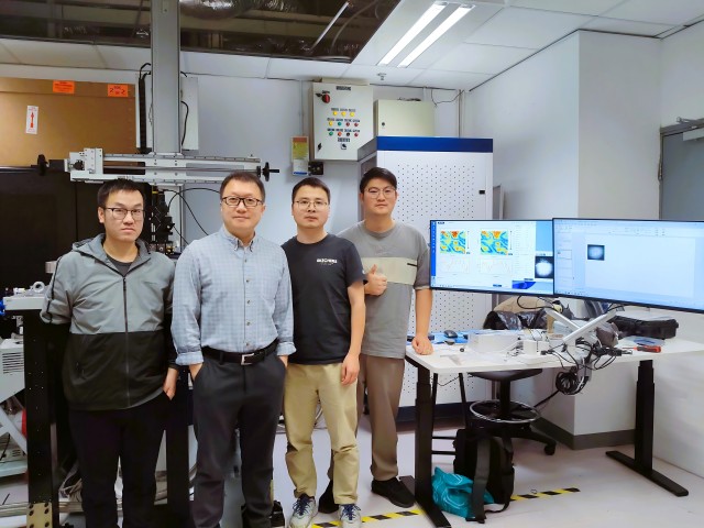
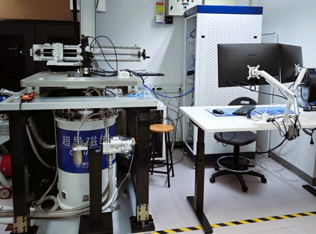
Recentlythe CIQTEK-developed Cryogenic Scanning Nitrogen-vacancy Microscope (SNVM) was successfully delivered to Professor Wong Chun-ling's research group at the City University of Hong Kong. This marks the broader recognition of CIQTEK's technical strength and service capability in the field of precision measurement.

Cryogenic Scanning Nitrogen-vacancy Microscope Delivered to City University of Hong Kong

Magnetism is one of the fundamental properties of materials, and the microscopic imaging of magnetism is an important direction in experimental physics research. By studying the microscopic magnetic properties of materials in depth, scientists can gain insights into the structure, electronic properties, and interactions of materials, which is of great significance for guiding the development of new magnetic storage materials and superconducting materials.

SNVM

The Cryogenic Scanning Nitrogen-vacancy Microscope is a precision measurement instrument that combines diamond NV center optical detection of magnetic resonance technology with atomic force microscopy scanning imaging technology. It can be used for high-resolution, high-sensitivity, quantitative, and non-destructive magnetic measurements in a wide temperature range of 2K to 300K. It has nanoscale spatial resolution and ultra-high detection sensitivity of single spins. It will provide a new approach for research in life sciences, materials science, condensed matter physics, and other fields.

City University of Hong Kong Header Photo

City University of Hong Kong is a public research university located in Hong Kong, renowned for its outstanding research and education in disciplines such as science, engineering, business, and law. Professor Wong Chun-ling's research group focuses on the study of two-dimensional and three-dimensional ferromagnetic and multiferroic materials and devices. By manipulating materials, and characterizing their structures and electrical/magnetic properties, the group aims to gain a deep understanding of the fundamental physics and unique properties of low-dimensional multiferroic materials and develop new materials/devices for the next generation of electronics and spintronics. The Cryogenic Scanning Nitrogen-vacancy Microscope will be an important scientific research tool in the field.


Maintaining a fusion splicer is crucial to ensure its optimal performance and extend its lifespan. Here are some general maintenance guidelines for a fusion splicer:


1. Regular Cleaning: Clean the fusion splicer after each use to remove dust, debris, and fiber residue. Use a soft, lint-free cloth and a mild cleaner specifically designed for fusion splicers. Avoid using solvents or abrasive materials that could damage the splicer's delicate components.


2. Electrode Inspection and Replacement: Check the electrodes regularly, as they degrade over time and can impact splicing quality. Follow the manufacturer's guidelines for electrode inspection and replacement intervals. If the electrodes are worn out or damaged, replace them with genuine electrodes recommended by the manufacturer.


3. Fiber Cleaver Maintenance: Clean the fiber cleaver regularly and make sure it is properly adjusted to obtain clean and precise cleaves. Check the blade condition and replace it if it becomes dull or chipped. Follow the manufacturer's instructions for cleaver maintenance.


4. Calibration and Alignment: Periodically calibrate and align the fusion splicer to ensure accurate splicing. Some splicers have an automated calibration feature, while others require manual adjustment. Follow the manufacturer's guidelines for calibration procedures.


5. Battery Maintenance: If your fusion splicer has a removable battery, properly charge and discharge it according to the manufacturer's instructions. Avoid overcharging or completely draining the battery, as it can reduce its lifespan. If the battery is built-in, follow the manufacturer's guidelines for maintenance.


6. Firmware Updates: Stay updated with the latest firmware releases for your fusion splicer. Manufacturers often provide firmware updates to improve performance, add features, or address known issues. Check the manufacturer's website periodically and follow the instructions for firmware updates.


7. Transport and Storage: When transporting the fusion splicer, use a protective case to prevent physical damage. Store the splicer in a clean and dry environment, away from excessive dust, moisture, and temperature extremes.


Professional Service: If you encounter any technical issues or experience a drop in splicing quality, consult the manufacturer's support documentation or contact their customer service for assistance. Some manufacturers provide authorized service centers for repairs and maintenance.

Polarization-Maintaining Fiber (PM Fiber) plays a vital role in various applications that require optimal signal integrity and polarization stability, such as telecommunications, fiber optic sensing, and laser systems. The use of a specialized Fusion Splicer for PM Fiber is essential to achieve accurate and reliable splicing, ensuring the preservation of the fiber’s polarization properties. This article explores the significance of a Polarization-Maintaining Fiber Fusion Splicer, its features, and its role in maintaining precise alignment for optical stability.
Understanding PM Fiber and its Challenges:


Polarization-Maintaining Fiber is designed to maintain the polarization state of light as it propagates through the fiber. Unlike conventional single-mode fiber, PM Fiber incorporates specific design elements that minimize polarization mode dispersion (PMD) and maximize polarization extinction ratio (PER). However, handling and splicing PM Fiber present unique challenges due to its polarization-sensitive nature.


Features of a Polarization-Maintaining Fiber Fusion Splicer:

Polarization-Maintaining Fiber Holders: These specialized holders are designed to securely hold the PM Fiber during the fusion splicing process. They ensure precise alignment of the polarization-maintaining fiber cores to maintain the desired polarization properties.

Precise Alignment Mechanism: The fusion splicer employs a sophisticated alignment mechanism that enables accurate alignment of the PM Fiber cores. It allows for precise control of the fiber position and angle, minimizing alignment errors and maximizing coupling efficiency.
Polarization Maintaining Splicing Modes: The fusion splicer provides dedicated splicing modes specifically designed for PM Fiber, ensuring optimal alignment of both the fiber cores and the polarization axes. These modes take into account the specific characteristics of PM Fiber, such as birefringence, to achieve optimal splicing results.

Real-Time Monitoring: The fusion splicer incorporates real-time monitoring capabilities, allowing technicians to monitor and adjust the alignment parameters during the splicing process. This ensures precise alignment and enables immediate feedback on splicing quality.


Importance of a Polarization-Maintaining Fiber Fusion Splicer:
Preservation of Polarization Properties: The precise alignment provided by the fusion splicer ensures the maintenance of the fiber's inherent polarization properties, such as PER and polarization extinction. This is crucial in applications where polarization stability is critical for optimal system performance.
Reduction of Insertion Loss and Crosstalk: Accurate alignment during fusion splicing minimizes insertion loss and crosstalk in PM Fiber connections. This ensures efficient transmission of polarized signals and reduces potential signal degradation.
Time and Cost Efficiency: The fusion splicer streamlines the splicing process, enabling quick and efficient splicing of PM Fiber. This saves time, reduces labor costs, and enhances productivity, especially in high-volume manufacturing or installation scenarios.

A Polarization-Maintaining Fiber Fusion Splicer is a critical tool for achieving precise alignment and reliable splicing of PM Fiber. By ensuring the preservation of polarization properties and reducing insertion loss and crosstalk, this specialized fusion splicer plays a vital role in maintaining optical stability and maximizing the performance of PM Fiber in various applications. With its advanced alignment mechanism and real-time monitoring capabilities, the fusion splicer enables efficient and accurate splicing, contributing to the seamless integration of PM Fiber in advanced optical systems technologies.